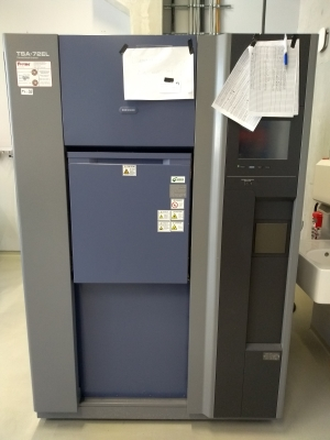
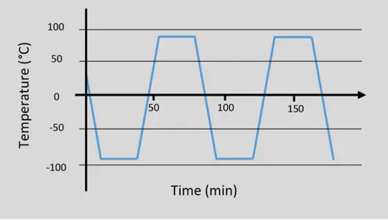
Electronic equipment can be subjected to many different types of temperature shock over a wide range of frequencies and acceleration levels. Temperature cycling and temperature shock testing in electronics packaging are used to determine the resistance of electronic devices to sudden exposure to extreme changes of temperature.
The primary goals are to qualify the electronic interconnect options for real environment applications and to establish the reliability and failure mechanisms. The main approach at our lab is to investigate the changes in the microstructure and evaluate the possible deterioration in the mechanical strength after exposure of the electronic devices to the thermal cycles and shocks. Therefore, we couple the thermal cycling tests with microstructural analysis techniques, shear testings, and strive to establish a correlation between the two.


![[Translate to English:] Logo Akkreditierungsrat: Systemakkreditiert](/fileadmin/_processed_/2/8/csm_AR-Siegel_Systemakkreditierung_bc4ea3377d.webp)


![[Translate to English:] Logo IHK Ausbildungsbetrieb 2023](/fileadmin/_processed_/6/0/csm_IHK_Ausbildungsbetrieb_digital_2023_6850f47537.webp)


